
|
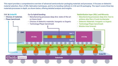
IDTechEx Explores Technology Trends in Dielectric Materials for Next Generation 2.5D and 3D Semiconductor Packaging
Wednesday, March 27, 2024
BOSTON, March 27, 2024 /PRNewswire/ -- The semiconductor industry continually pushes packaging technology boundaries to meet the demand for higher chip performance and efficiency. Bandwidth is one of the critical factors defining the amount of data transmitted between dies on a package. Bandwidth, crucial for communication speed and efficiency, is impacted by factors such as IO/mm and Datarate/IO, which are, in turn, influenced by the dielectric materials selected for 2.5D and 3D packaging. This article explores the technology trends in dielectric materials for both 2.5D and 3D packaging, with insights drawn from IDTechEx's market report on the topic, "Materials and Processing for Advanced Semiconductor Packaging 2024-2034".
2.5D packaging:
For 2.5D packaging, achieving high bandwidth relies on the redistribution layer (RDL) within the package, where features like Line/Space (L/S), via, and pad dimensions are important. However, traditional inorganic dielectric materials like SiO(2), though capable of achieving fine L/S, suffer from high dielectric constants (Dk=3.9) and are tied to the Si manufacturing technique. This hinders high-speed communication and presents costly challenges. Consequently, researchers are exploring organic alternatives with lower dielectric constants to enhance performance and reduce costs.
Organic dielectric materials emerge as promising alternatives for advanced semiconductor packaging, offering lower dielectric constants and cost advantages. However, selecting suitable organic dielectrics demands careful consideration of key parameters. IDTechEx's "Materials and Processing for Advanced Semiconductor Packaging 2024-2034" report identifies five critical parameters crucial for organic dielectrics, including Dk (dielectric constant) and Df (loss tangent), CTE (Coefficient of Thermal Expansion), Elongation, Young's modulus, and Moisture absorption. Ideally, one would expect to have materials that exhibit low Dk and Df, compatible CTE with Si and Cu, high elongation value, and a moderate Young's modulus to provide stability to the package. However, material selection entails trade-offs; for example, low Dk polymers may exhibit higher coefficients of thermal expansion (CTE), impacting device reliability and packaging architectures. Thus, achieving a balance among these parameters is critical for successful material selection in semiconductor packaging.
3D packaging:
Reducing the pitches between solder bumps has been a continuous advancement in the evolution of 3D packaging. However, such an approach presents challenges in establishing reliable electrical connections due to reduced bump height and surface area, necessitating precise manufacturing processes. Thermocompression Bonding (TCB) addresses this by enabling fine-pitch bonding as small as 10 m, although issues such as Intermetallic Compound (IMC) formation and solder ball bridging persist. To overcome these challenges, Cu-Cu Hybrid Bonding technology embeds metal contacts between dielectric materials and employs heat treatment for copper atom diffusion, eliminating soldering-related bridging problems and enhancing reliability in high-performance component packaging. It is considered a promising solution for the semiconductor industry, pushing the boundaries of miniaturization and performance in electronic devices.
Currently, hybrid bonding relies on inorganic dielectric materials like SiO2 or SiCN for insulation, which struggle with achieving fine-scale topography patterns and demand front-end manufacturing techniques. Alternatively, organic dielectrics, akin to the benefit it brings to 2.5D packaging, offer benefits such as low-k properties, reducing RC delay and insertion loss, resisting Cu migration, and tolerating defects and warpage better. However, using organic dielectrics for 3D hybrid bonding is still in the R&D phase due to challenges like elevated bonding temperatures (memory applications limit the bonding temperature to be below 250°C and in certain applications (such as displays) that contain sensitive materials embedded in the deck that cannot sustain high temperatures, the bonding temperature requirement must be reduced to 150°C. Furthermore, CMP compatibility with polymers remains a critical issue. Half-cured polymer's characteristics, including low modulus, viscoelastic behavior, and adhesion, pose challenges for ensuring Cu surface reliability during CMP. Modulus differences between Cu and polymer further complicate Cu protrusion formation.
IDTechEx's "Materials and Processing for Advanced Semiconductor Packaging 2024-2034" report suggests that if their properties are enhanced, organic dielectrics may become viable for hybrid bonding. If successful, integrating organic materials into mass production processes could prompt OSAT companies to adopt hybrid bonding more widely. This shift could broaden the technology's availability beyond a few foundries, as organic dielectrics offer the potential to ease stringent manufacturing and cleanroom standards associated with inorganic materials.
The report offers a structured overview of advanced semiconductor packaging in four main sections. The first part covers technology, trends, applications, and the ecosystem. The second part delves into 2.5D packaging processes, exploring dielectric materials, RDL fabrication, and material selection. Detailed analyses, player evaluations, and future trends are provided. Moving beyond 2.5D, the third part focuses on Cu-Cu hybrid bonding for 3D die stacking, offering insights into manufacturing processes, material selection, and case studies. Finally, the report includes a 10-year market forecast for Organic Dielectric Advanced Semiconductor Packaging, providing industry perspectives on market growth and trends.
To find out more about this report, including downloadable sample pages, please visit www.IDTechEx.com/MatsforASP.
For the full portfolio of semiconductor market research from IDTechEx, please see www.IDTechEx.com/Research/Semiconductors.
About IDTechEx:
IDTechEx provides trusted independent research on emerging technologies and their markets. Since 1999, we have been helping our clients to understand new technologies, their supply chains, market requirements, opportunities and forecasts. For more information, contact research@IDTechEx.com or visit www.IDTechEx.com.
Image Download:
https://www.dropbox.com/scl/fo/2hli4xkr16e69kxz67val/h?rlkey=xxzpspi28rk9nzueeya8tld3d&dl=0
Photo: https://mma.prnewswire.com/media/2373227/Scope_IDTechEx.jpg
Logo: https://mma.prnewswire.com/media/478371/4617637/IDTechEx_Logo.jpg
Media Contact:
Lucy Rogers
Sales and Marketing Administrator
press@IDTechEx.com
+44(0)1223 812300
Social Media Links:
Twitter: www.twitter.com/IDTechEx
LinkedIn: www.linkedin.com/company/IDTechEx
View original content to download multimedia:https://www.prnewswire.com/news-releases/idtechex-explores-technology-trends-in-dielectric-materials-for-next-generation-2-5d-and-3d-semiconductor-packaging-302100954.html
SOURCE IDTechEx
|
|
|
|
|
|
 |
Energy Toolbase Launches Energy Storage Partnership with Sungrow to Support PowerStack 255CS and PowerTitan 2.0 | Jan 22, 2026
|
|
RS now offers Phoenix Contact's pioneering new NearFi technology | Jan 22, 2026
|
|
MetaOptics to Showcase Five Breakthrough Metalens-Powered Products at CES 2026 | Jan 22, 2026
|
|
Quantum Art Raises $100 Million in Series A Round to Drive Scalable, Multi-Core Quantum Computing | Jan 22, 2026
|
|
SCAILIUM Debuts "AI Production Layer" to Overcome GPU Starvation and Slash AI Energy Waste | Jan 22, 2026
|
|
Fresco Raises EUR15m Series C to Power the Future of AI-Driven Cooking and the Connected Kitchen Ecosystem | Jan 22, 2026
|
|
Einride and IonQ Partnership Uses Quantum Computing to Optimize the Logistics of Electric and Autonomous Freight | Jan 22, 2026
|
|
No Assembly Required: Barrett Distribution Centers Powers Maxwood Furniture's West Coast DTC Expansion | Jan 22, 2026
|
|
Hesai Recognized as the Only Lidar Company on Morgan Stanley's "Humanoid Tech 25" of Global Robotics Leaders | Jan 22, 2026
|
|
Ekinops New C700HC Chassis Efficiently Connects the Data Center and the Central Office | Jan 22, 2026
|
|
|
|


