NEO Semiconductor Introduces World's First Extreme High Bandwidth Memory (X-HBM) Architecture for AI Chips
Wednesday, August 13, 2025
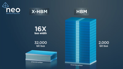
New X-HBM architecture delivers a 32K-bit wide data bus and potentially 512 Gbit per die density, offering 16X more bandwidth or 10X higher density than traditional HBM
SAN JOSE, Calif., Aug. 5, 2025 /PRNewswire/ -- NEO Semiconductor, a leading developer of breakthrough memory technologies, today introduced the world's first Extreme High Bandwidth Memory (X-HBM) architecture for AI chips. Built to meet the growing demands of generative AI and high-performance computing, X-HBM delivers unmatched performance with a 32K-bit data bus and potentially 512 Gbit per die, dramatically surpassing the limitations of traditional HBM with 16X greater bandwidth or 10X higher density.
"X-HBM is not an incremental upgrade, it's a fundamental breakthrough," said Andy Hsu, Founder & CEO of NEO Semiconductor. "With 16X the bandwidth or 10X the density of current memory technologies, X-HBM gives AI chipmakers a clear path to deliver next-generation performance years ahead of the existing roadmap. It's a game-changer for accelerating AI infrastructure, reducing energy consumption, and scaling AI capabilities across industries."
Built on NEO's proprietary 3D X-DRAM architecture, X-HBM represents a major leap in memory technology by eliminating long-standing limitations in bandwidth and density. In contrast, HBM5, still in development and expected to reach the market around 2030, is projected to support only 4K-bit data buses and 40 Gbit per die. A recent study from the Korea Advanced Institute of Science and Technology (KAIST) projects that even HBM8, expected around 2040, will offer just 16K-bit buses and 80 Gbit per die. In comparison, X-HBM delivers 32K-bit buses and 512 Gbit per die, allowing AI chip designers to bypass a full decade of incremental performance bottlenecks associated with traditional HBM technology.
Key Features and Benefits:
    --  Scalable - Enables faster data transfer between GPUs and memory for more
        efficient AI scaling.
    --  High-Performance - Unlocks untapped GPU capabilities to boost AI
        workloads.
    --  Sustainable - Reduces power and hardware needs by consolidating AI
        infrastructure.
NEO Semiconductor's CEO, Andy Hsu, will deliver a keynote presentation on August 6, at 11 a.m. PST at FMS: the Future of Memory and Storage, where he will discuss the breakthrough X-HBM technology. The event takes place August 5-7, 2025, at the Santa Clara Convention Center in California, USA. NEO Semiconductor will also be exhibiting at booth #507. To schedule a meeting at FMS 2025, please contact: mayalustig@neosemic.com.
About NEO Semiconductor
NEO Semiconductor is a high-tech company pioneering next-generation memory technologies, including 3D NAND flash, 3D DRAM, and 3D AI solutions. Founded in 2012 by Andy Hsu in San Jose, California, the company holds over 30 U.S. patents. NEO's key innovations include X-NAND(TM), which delivers SLC performance from TLC and QLC memory, and X-DRAM(TM), the world's lowest-power DRAM architecture. In 2023, NEO introduced 3D X-DRAM(TM), the first DRAM built on a 3D NAND-like structure to overcome the scaling limits of conventional DRAM. In 2024, the company unveiled 3D X-AI(TM), a breakthrough architecture designed to accelerate AI performance and efficiency. For more information, visit https://neosemic.com.
Photo - https://mma.prnewswire.com/media/2743404/NEO_Semiconductor_X_HBM.jpg
Logo - https://mma.prnewswire.com/media/2680564/NEO_Semiconductor_Logo.jpg
Media and Analyst Contact:
Maya Lustig
mayalustig@neosemic.com
View original content to download multimedia:https://www.prnewswire.com/news-releases/neo-semiconductor-introduces-worlds-first-extreme-high-bandwidth-memory-x-hbm-architecture-for-ai-chips-302521977.html
SOURCE NEO Semiconductor
|
|

|
|
|
 |
Energy Toolbase Launches Energy Storage Partnership with Sungrow to Support PowerStack 255CS and PowerTitan 2.0 | Jan 22, 2026
|
|
RS now offers Phoenix Contact's pioneering new NearFi technology | Jan 22, 2026
|
|
SCAILIUM Debuts "AI Production Layer" to Overcome GPU Starvation and Slash AI Energy Waste | Jan 22, 2026
|
|
Einride and IonQ Partnership Uses Quantum Computing to Optimize the Logistics of Electric and Autonomous Freight | Jan 22, 2026
|
|
MetaOptics to Showcase Five Breakthrough Metalens-Powered Products at CES 2026 | Jan 22, 2026
|
|
Quantum Art Raises $100 Million in Series A Round to Drive Scalable, Multi-Core Quantum Computing | Jan 22, 2026
|
|
No Assembly Required: Barrett Distribution Centers Powers Maxwood Furniture's West Coast DTC Expansion | Jan 22, 2026
|
|
Hesai Recognized as the Only Lidar Company on Morgan Stanley's "Humanoid Tech 25" of Global Robotics Leaders | Jan 22, 2026
|
|
Fresco Raises EUR15m Series C to Power the Future of AI-Driven Cooking and the Connected Kitchen Ecosystem | Jan 22, 2026
|
|
Cellid and Jig.jp Jointly Develop AR Glasses | Jan 22, 2026
|
|
|


